Da ta S h ee t, D S 1, N ov . 20 01
T - S M I NT O
4B3 T S e co n d G e n .
M od ul ar I S D N N T
( O r din a ry )
PEF 80902 Version 1.1
Wired
C o m m u n i ca t i o n s
N e v e r
s t o p
t h i n k i n g .
�Edition 2001-11-12
Published by Infineon Technologies AG,
St.-Martin-Strasse 53,
D-81541 München, Germany
© Infineon Technologies AG 2001.
All Rights Reserved.
Attention please!
The information herein is given to describe certain components and shall not be considered as warranted
characteristics.
Terms of delivery and rights to technical change reserved.
We hereby disclaim any and all warranties, including but not limited to warranties of non-infringement, regarding
circuits, descriptions and charts stated herein.
Infineon Technologies is an approved CECC manufacturer.
Information
For further information on technology, delivery terms and conditions and prices please contact your nearest
Infineon Technologies Office in Germany or our Infineon Technologies Representatives worldwide (see address
list).
Warnings
Due to technical requirements components may contain dangerous substances. For information on the types in
question please contact your nearest Infineon Technologies Office.
Infineon Technologies Components may only be used in life-support devices or systems with the express written
approval of Infineon Technologies, if a failure of such components can reasonably be expected to cause the failure
of that life-support device or system, or to affect the safety or effectiveness of that device or system. Life support
devices or systems are intended to be implanted in the human body, or to support and/or maintain and sustain
and/or protect human life. If they fail, it is reasonable to assume that the health of the user or other persons may
be endangered.
�Da ta S h ee t, D S 1, N ov . 20 01
T - S M I NT O
4B3 T S e co n d G e n .
M od ul ar I S D N N T
( O r din a ry )
PEF 80902 Version 1.1
Wired
C o m m u n i ca t i o n s
N e v e r
s t o p
t h i n k i n g .
�PEF 80902
Revision History:
2001-11-12
Previous Version:
Preliminary Data Sheet 06.01
Page
DS 1
Subjects (major changes since last revision)
Table 10
Additional C/I-command LTD
Figure 12
Chapter 2.3.7.4
Chapter 4.2
Input Leakage Current AIN, BIN: max. 30µA
Chapter 4.4
Reduced power consumption
For questions on technology, delivery and prices please contact the Infineon
Technologies Offices in Germany or the Infineon Technologies Companies and
Representatives worldwide: see our webpage at http://www.infineon.com
�PEF 80902
Table of Contents
Page
1
1.1
1.2
1.3
1.4
1.5
1.6
1.6.1
1.7
Overview . . . . . . . . . . . . . . . . . . . . . . . . . . . . . . . . . . . . . . . . . . . . . . . . . . . 1
References . . . . . . . . . . . . . . . . . . . . . . . . . . . . . . . . . . . . . . . . . . . . . . . . . 2
Features . . . . . . . . . . . . . . . . . . . . . . . . . . . . . . . . . . . . . . . . . . . . . . . . . . . . 3
Not Supported are ... . . . . . . . . . . . . . . . . . . . . . . . . . . . . . . . . . . . . . . . . . . 4
Pin Configuration . . . . . . . . . . . . . . . . . . . . . . . . . . . . . . . . . . . . . . . . . . . . . 5
Block Diagram . . . . . . . . . . . . . . . . . . . . . . . . . . . . . . . . . . . . . . . . . . . . . . . 6
Pin Definitions and Functions . . . . . . . . . . . . . . . . . . . . . . . . . . . . . . . . . . . 7
Specific Pins and Test Modes . . . . . . . . . . . . . . . . . . . . . . . . . . . . . . . . . 9
System Integration . . . . . . . . . . . . . . . . . . . . . . . . . . . . . . . . . . . . . . . . . . . 11
2
2.1
2.2
2.2.1
2.3
2.3.1
2.3.2
2.3.3
2.3.4
2.3.4.1
2.3.5
2.3.6
2.3.7
2.3.7.1
2.3.7.2
2.3.7.3
2.3.7.4
2.3.7.5
2.3.7.6
2.4
2.4.1
2.4.2
2.4.3
2.4.4
2.4.5
2.4.5.1
Functional Description . . . . . . . . . . . . . . . . . . . . . . . . . . . . . . . . . . . . . .
Reset Generation . . . . . . . . . . . . . . . . . . . . . . . . . . . . . . . . . . . . . . . . . . . .
IOM-2 Interface . . . . . . . . . . . . . . . . . . . . . . . . . . . . . . . . . . . . . . . . . . . .
IOM‚-2 Functional Description . . . . . . . . . . . . . . . . . . . . . . . . . . . . . . . .
U-Transceiver . . . . . . . . . . . . . . . . . . . . . . . . . . . . . . . . . . . . . . . . . . . . . .
4B3T Frame Structure . . . . . . . . . . . . . . . . . . . . . . . . . . . . . . . . . . . . . .
Maintenance Channel . . . . . . . . . . . . . . . . . . . . . . . . . . . . . . . . . . . . . .
Coding from Binary to Ternary Data . . . . . . . . . . . . . . . . . . . . . . . . . . .
Decoding from Ternary to Binary Data . . . . . . . . . . . . . . . . . . . . . . . . .
Monitoring of Code Violations . . . . . . . . . . . . . . . . . . . . . . . . . . . . . .
Scrambler / Descrambler . . . . . . . . . . . . . . . . . . . . . . . . . . . . . . . . . . . .
Command/Indication Codes . . . . . . . . . . . . . . . . . . . . . . . . . . . . . . . . .
State Machine for Activation and Deactivation . . . . . . . . . . . . . . . . . . .
State Machine Notation . . . . . . . . . . . . . . . . . . . . . . . . . . . . . . . . . . .
Awake Protocol . . . . . . . . . . . . . . . . . . . . . . . . . . . . . . . . . . . . . . . . .
NT State Machine (IEC-T / NTC-T Compatible) . . . . . . . . . . . . . . . .
Inputs to the U-Transceiver . . . . . . . . . . . . . . . . . . . . . . . . . . . . . . . .
Outputs of the U-Transceiver . . . . . . . . . . . . . . . . . . . . . . . . . . . . . . .
NT-States . . . . . . . . . . . . . . . . . . . . . . . . . . . . . . . . . . . . . . . . . . . . . .
S-Transceiver . . . . . . . . . . . . . . . . . . . . . . . . . . . . . . . . . . . . . . . . . . . . . .
Line Coding, Frame Structure . . . . . . . . . . . . . . . . . . . . . . . . . . . . . . . .
S/Q Channels, Multiframing . . . . . . . . . . . . . . . . . . . . . . . . . . . . . . . . . .
Data Transfer between IOM‚-2 and S0 . . . . . . . . . . . . . . . . . . . . . . . . .
Loopback 2 . . . . . . . . . . . . . . . . . . . . . . . . . . . . . . . . . . . . . . . . . . . . . .
State Machine . . . . . . . . . . . . . . . . . . . . . . . . . . . . . . . . . . . . . . . . . . . .
State Machine NT Mode . . . . . . . . . . . . . . . . . . . . . . . . . . . . . . . . . .
13
13
14
14
15
15
19
19
20
21
21
22
23
23
24
26
27
29
30
33
33
34
35
35
35
38
3
3.1
3.1.1
3.1.2
3.1.3
3.1.4
Operational Description . . . . . . . . . . . . . . . . . . . . . . . . . . . . . . . . . . . . .
Layer 1 Activation/Deactivation . . . . . . . . . . . . . . . . . . . . . . . . . . . . . . . . .
Generation of 4B3T Signal Elements . . . . . . . . . . . . . . . . . . . . . . . . . .
Complete Activation Initiated by Exchange . . . . . . . . . . . . . . . . . . . . . .
Complete Activation Initiated by TE . . . . . . . . . . . . . . . . . . . . . . . . . . . .
Deactivation . . . . . . . . . . . . . . . . . . . . . . . . . . . . . . . . . . . . . . . . . . . . . .
42
42
42
45
46
47
Data Sheet
2001-11-12
�PEF 80902
Table of Contents
Page
3.1.5
3.2
3.2.1
3.2.1.1
3.3
3.3.1
3.3.2
3.3.3
3.3.4
3.3.5
Activation Procedures with Loopback #2 . . . . . . . . . . . . . . . . . . . . . . . .
Layer 1 Loopbacks . . . . . . . . . . . . . . . . . . . . . . . . . . . . . . . . . . . . . . . . . .
Loopback No.2 . . . . . . . . . . . . . . . . . . . . . . . . . . . . . . . . . . . . . . . . . . . .
Complete Loopback . . . . . . . . . . . . . . . . . . . . . . . . . . . . . . . . . . . . . .
External Circuitry . . . . . . . . . . . . . . . . . . . . . . . . . . . . . . . . . . . . . . . . . . . .
Power Supply Blocking Recommendation . . . . . . . . . . . . . . . . . . . . . . .
U-Transceiver . . . . . . . . . . . . . . . . . . . . . . . . . . . . . . . . . . . . . . . . . . . .
S-Transceiver . . . . . . . . . . . . . . . . . . . . . . . . . . . . . . . . . . . . . . . . . . . .
Oscillator Circuitry . . . . . . . . . . . . . . . . . . . . . . . . . . . . . . . . . . . . . . . . .
General . . . . . . . . . . . . . . . . . . . . . . . . . . . . . . . . . . . . . . . . . . . . . . . . .
48
49
49
49
50
50
50
52
55
55
4
4.1
4.2
4.3
4.4
4.5
4.6
4.6.1
4.6.2
4.6.3
Electrical Characteristics . . . . . . . . . . . . . . . . . . . . . . . . . . . . . . . . . . . .
Absolute Maximum Ratings . . . . . . . . . . . . . . . . . . . . . . . . . . . . . . . . . . . .
DC Characteristics . . . . . . . . . . . . . . . . . . . . . . . . . . . . . . . . . . . . . . . . . . .
Capacitances . . . . . . . . . . . . . . . . . . . . . . . . . . . . . . . . . . . . . . . . . . . . . . .
Power Consumption . . . . . . . . . . . . . . . . . . . . . . . . . . . . . . . . . . . . . . . . .
Supply Voltages . . . . . . . . . . . . . . . . . . . . . . . . . . . . . . . . . . . . . . . . . . . . .
AC Characteristics . . . . . . . . . . . . . . . . . . . . . . . . . . . . . . . . . . . . . . . . . . .
IOM-2 Interface . . . . . . . . . . . . . . . . . . . . . . . . . . . . . . . . . . . . . . . . . . .
Reset . . . . . . . . . . . . . . . . . . . . . . . . . . . . . . . . . . . . . . . . . . . . . . . . . . .
Undervoltage Detection Characteristics . . . . . . . . . . . . . . . . . . . . . . . .
56
56
57
59
59
59
61
62
64
65
5
Package Outlines . . . . . . . . . . . . . . . . . . . . . . . . . . . . . . . . . . . . . . . . . . . 67
6
6.1
6.1.1
6.1.2
6.2
6.2.1
6.2.2
6.2.3
6.3
Appendix: Differences between Q- and T-SMINT‚O . . . . . . . . . . . . . . .
Pinning . . . . . . . . . . . . . . . . . . . . . . . . . . . . . . . . . . . . . . . . . . . . . . . . . . . .
Pin Definitions and Functions . . . . . . . . . . . . . . . . . . . . . . . . . . . . . . . .
LED Pin ACT . . . . . . . . . . . . . . . . . . . . . . . . . . . . . . . . . . . . . . . . . . . . .
U-Transceiver . . . . . . . . . . . . . . . . . . . . . . . . . . . . . . . . . . . . . . . . . . . . . .
U-Interface Conformity . . . . . . . . . . . . . . . . . . . . . . . . . . . . . . . . . . . . . .
U-Transceiver State Machines . . . . . . . . . . . . . . . . . . . . . . . . . . . . . . .
Command/Indication Codes . . . . . . . . . . . . . . . . . . . . . . . . . . . . . . . . .
External Circuitry . . . . . . . . . . . . . . . . . . . . . . . . . . . . . . . . . . . . . . . . . . . .
7
Index . . . . . . . . . . . . . . . . . . . . . . . . . . . . . . . . . . . . . . . . . . . . . . . . . . . . . 74
Data Sheet
68
68
68
68
69
69
70
72
73
2001-11-12
�PEF 80902
List of Figures
Page
Figure 1
Figure 2
Figure 3
Figure 4
Figure 5
Figure 6
Figure 7
Figure 8
Figure 9
Figure 10
Figure 11
Figure 12
Figure 13
Figure 14
Figure 15
Figure 16
Figure 17
Figure 18
Figure 19
Figure 20
Figure 21
Figure 22
Figure 23
Figure 24
Figure 25
Figure 26
Figure 27
Figure 28
Figure 29
Figure 30
Figure 31
Pin Configuration . . . . . . . . . . . . . . . . . . . . . . . . . . . . . . . . . . . . . . . . . . 5
Block Diagram . . . . . . . . . . . . . . . . . . . . . . . . . . . . . . . . . . . . . . . . . . . . 6
Application Example T-SMINT‚O: Standard NT1 . . . . . . . . . . . . . . . . . 12
IOM-2 Frame Structure of the T-SMINT‚O . . . . . . . . . . . . . . . . . . . . 14
State Diagram Example . . . . . . . . . . . . . . . . . . . . . . . . . . . . . . . . . . . . 23
Awake Procedure initiated by the LT . . . . . . . . . . . . . . . . . . . . . . . . . . 24
Awake Procedure initiated by the NT. . . . . . . . . . . . . . . . . . . . . . . . . . 24
NT State Machine (IEC-T/NTC-T Compatible). . . . . . . . . . . . . . . . . . . 26
S/T -Interface Line Code . . . . . . . . . . . . . . . . . . . . . . . . . . . . . . . . . . . 33
Frame Structure at Reference Points S and T (ITU I.430). . . . . . . . . . 34
State Diagram Notation . . . . . . . . . . . . . . . . . . . . . . . . . . . . . . . . . . . . 36
State Machine NT Mode . . . . . . . . . . . . . . . . . . . . . . . . . . . . . . . . . . . 38
Activation Initiated by Exchange . . . . . . . . . . . . . . . . . . . . . . . . . . . . . 45
Activation Initiated by TE . . . . . . . . . . . . . . . . . . . . . . . . . . . . . . . . . . . 46
Deactivation (always Initiated by LT) . . . . . . . . . . . . . . . . . . . . . . . . . . 47
Activation of Loopback #2 . . . . . . . . . . . . . . . . . . . . . . . . . . . . . . . . . . 48
Test Loopbacks . . . . . . . . . . . . . . . . . . . . . . . . . . . . . . . . . . . . . . . . . . 49
Power Supply Blocking . . . . . . . . . . . . . . . . . . . . . . . . . . . . . . . . . . . . 50
External Circuitry U-Transceiver with External Hybrid . . . . . . . . . . . . . 51
External Circuitry S-Interface Transmitter . . . . . . . . . . . . . . . . . . . . . . 54
External Circuitry S-Interface Receiver . . . . . . . . . . . . . . . . . . . . . . . . 54
Crystal Oscillator . . . . . . . . . . . . . . . . . . . . . . . . . . . . . . . . . . . . . . . . . 55
Maximum Sinusoidal Ripple on Supply Voltage . . . . . . . . . . . . . . . . 60
Input/Output Waveform for AC Tests. . . . . . . . . . . . . . . . . . . . . . . . . . 61
IOM®-2 Interface - Bit Synchronization Timing . . . . . . . . . . . . . . . . . . 62
IOM-2 Interface - Frame Synchronization Timing . . . . . . . . . . . . . . . . 62
Reset Input Signal . . . . . . . . . . . . . . . . . . . . . . . . . . . . . . . . . . . . . . . . 64
Undervoltage Control Timing . . . . . . . . . . . . . . . . . . . . . . . . . . . . . . . . 65
NTC-Q Compatible State Machine Q-SMINT‚O: 2B1Q . . . . . . . . . . . . 70
IEC-T/NTC-T Compatible State Machine T-SMINT‚O: 4B3T . . . . . . . . 71
External Circuitry Q- and T-SMINT‚O . . . . . . . . . . . . . . . . . . . . . . . . . 73
Data Sheet
2001-11-12
�PEF 80902
List of Tables
Table 1
Table 2
Table 3
Table 4
Table 5
Table 6
Table 7
Table 8
Table 9
Table 10
Table 11
Table 12
Table 13
Table 14
Table 15
Table 16
Table 17
Table 18
Table 19
Table 20
Table 21
Table 22
Table 23
Table 24
Table 25
Table 26
Table 27
Table 28
Table 29
Table 30
Table 31
Table 32
Table 33
Data Sheet
Page
NT Products of the 2nd Generation . . . . . . . . . . . . . . . . . . . . . . . . . . . . 1
Pin Definitions and Functions . . . . . . . . . . . . . . . . . . . . . . . . . . . . . . . . 7
ACT States. . . . . . . . . . . . . . . . . . . . . . . . . . . . . . . . . . . . . . . . . . . . . . 10
LP2I States . . . . . . . . . . . . . . . . . . . . . . . . . . . . . . . . . . . . . . . . . . . . . 10
Test Modes . . . . . . . . . . . . . . . . . . . . . . . . . . . . . . . . . . . . . . . . . . . . . 10
Frame Structure A for Downstream Transmission LT to NT . . . . . . . . 16
Frame Structure B for Upstream Transmission NT to LT. . . . . . . . . . . 18
MMS 43 Coding Table . . . . . . . . . . . . . . . . . . . . . . . . . . . . . . . . . . . . . 19
4B3T Decoding Table . . . . . . . . . . . . . . . . . . . . . . . . . . . . . . . . . . . . . 20
C/I Codes . . . . . . . . . . . . . . . . . . . . . . . . . . . . . . . . . . . . . . . . . . . . . . . 22
Differences to the former NT-SM of the IEC-T/NTC-T . . . . . . . . . . . . . 27
Timers . . . . . . . . . . . . . . . . . . . . . . . . . . . . . . . . . . . . . . . . . . . . . . . . . 28
Active States . . . . . . . . . . . . . . . . . . . . . . . . . . . . . . . . . . . . . . . . . . . . 30
M Symbol Output . . . . . . . . . . . . . . . . . . . . . . . . . . . . . . . . . . . . . . . . . 30
Signal Output on Uk0 in State Test . . . . . . . . . . . . . . . . . . . . . . . . . . . 30
C/I-Code Output. . . . . . . . . . . . . . . . . . . . . . . . . . . . . . . . . . . . . . . . . . 30
4B3T Signal Elements . . . . . . . . . . . . . . . . . . . . . . . . . . . . . . . . . . . . . 42
Generation of the 4B3T Signal Elements. . . . . . . . . . . . . . . . . . . . . . . 43
S/T-Interface Signals . . . . . . . . . . . . . . . . . . . . . . . . . . . . . . . . . . . . . . 44
U-Transformer Parameters . . . . . . . . . . . . . . . . . . . . . . . . . . . . . . . . . 51
S-Transformer Parameters . . . . . . . . . . . . . . . . . . . . . . . . . . . . . . . . . 53
Crystal Parameters . . . . . . . . . . . . . . . . . . . . . . . . . . . . . . . . . . . . . . . 55
Maximum Input Currents . . . . . . . . . . . . . . . . . . . . . . . . . . . . . . . . . . . 56
S-Transceiver Characteristics . . . . . . . . . . . . . . . . . . . . . . . . . . . . . . . 57
U-Transceiver Characteristics . . . . . . . . . . . . . . . . . . . . . . . . . . . . . . . 58
Pin Capacitances . . . . . . . . . . . . . . . . . . . . . . . . . . . . . . . . . . . . . . . . . 59
Reset Input Signal Characteristics. . . . . . . . . . . . . . . . . . . . . . . . . . . . 64
Parameters of the UVD/POR Circuit . . . . . . . . . . . . . . . . . . . . . . . . . . 65
Pin Definitions and Functions . . . . . . . . . . . . . . . . . . . . . . . . . . . . . . . 68
ACT States. . . . . . . . . . . . . . . . . . . . . . . . . . . . . . . . . . . . . . . . . . . . . . 68
Related Documents to the U-Interface. . . . . . . . . . . . . . . . . . . . . . . . . 69
C/I Codes . . . . . . . . . . . . . . . . . . . . . . . . . . . . . . . . . . . . . . . . . . . . . . . 72
Dimensions of External Components. . . . . . . . . . . . . . . . . . . . . . . . . . 73
2001-11-12
�PEF 80902
Overview
1
Overview
The PEB 80902 (T-SMINTâO) offers all NT1 features known from the PEB 8090 [9] and
can hence replace the latter in all NT1 applications.
Table 1 on Page 1 summarizes the 2nd generation NT products.
•
Table 1
NT Products of the 2nd Generation
PEF 80902
®
PEF 81902
PEF 82902
T-SMINT O
T-SMINT IX
T-SMINT®I
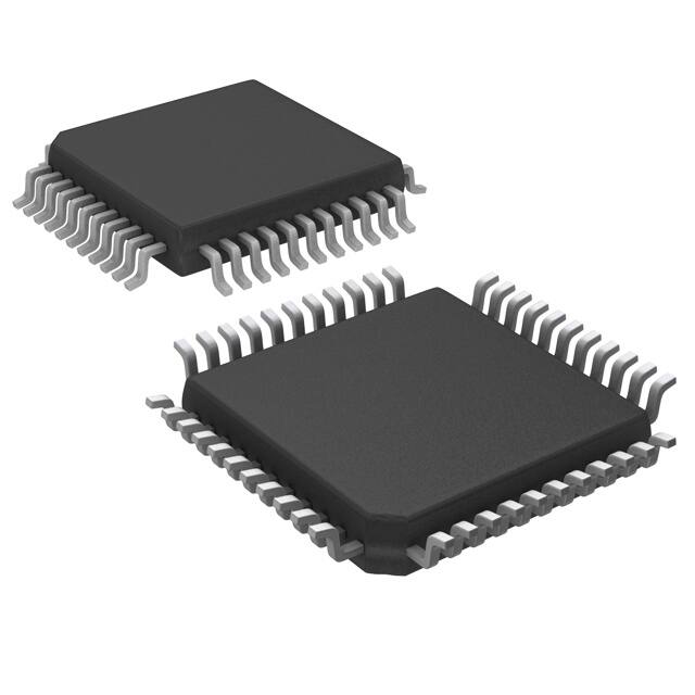
Package
P-MQFP-44
P-MQFP-64
P-TQFP-64
P-MQFP-64
P-TQFP-64
Register
access
no
U+S+HDLC+ IOMâ−2
U+S+IOMâ−2
Access via
n.a
MCLK,
watchdog timer,
SDS, BCL, Dchannel
arbitration,
IOMâ−2 access
and
manipulation
etc. provided
no
yes
yes
HDLC
controller
no
yes
no
NT1 mode
available
yes (only)
no
no
Data Sheet
®
parallel (or SCI or IOMâ−2) parallel (or SCI or IOMâ−2)
1
2001-11-12
�PEF 80902
Overview
1.1
References
[1]
TS 102 080, Transmission and Multiplexing; ISDN basic rate access; Digital
transmission system on metallic local lines, ETSI, November 1998
[2]
FTZ 1 TR 220 Technische Richtlinie, Spezifikation der ISDN Schnittstelle
Uk0 Schicht 1, Deutsche Telecom AG, August 1991
[3]
TS 0284/96 Technische Spezifikation Intelligenter Netzabschluß (iNT) mit
den Funktionen eines Terminaladapters TA 2a/b (ohne Internverkehr),
Deutsche Telekom AG, März 2001
[4]
pr ETS 300 012 Draft, ISDN; Basic User Network Interface (UNI), ETSI,
November 1996
[5]
T1.605-1991, ISDN-Basic Access Interface for S and T Reference Points
(Layer 1 Specification), ANSI, 1991
[6]
I.430, ISDN User-Network Interfaces: Layer 1 Recommendations, ITU,
November 1988
[7]
IEC-T, ISDN Echocancellation Circuit, PEB 20901 (IEC - TD) / PEB 20902
(IEC - TA), preliminary Target Specification 11.88, Siemens AG, 1988
[8]
SBCX, S/T Bus Interface Circuit Extended, PEB 2081 V3.4, User’s Manual
11.96, Siemens AG, 1996
[9]
NTC-T, Network Termination Controller (4B3T), PEB 8090 V1.1, Data Sheet
06.98, Siemens AG, 1998
[10]
INTC-Q, Intelligent Network Termination Controller (2B1Q), PEB 8191 V1.1,
Data Sheet 10.97, Siemens AG, 1997
[11]
Q-SMINTO, 2B1Q Second Gen. Modular ISDN NT (Ordinary), PEF 80912
Q-SMINTIX, 2B1Q Second Gen. Modular ISDN NT (Intelligent eXended),
PEF 81912
Q-SMINTI, 2B1Q Second Gen. Modular ISDN NT (Intelligent), PEF 82912
V1.3, Data Sheets 03.01, Infineon AG, 2001
[12]
IOMâ-2 Interface Reference Guide, Siemens AG, 03.91
[13]
SCOUT-S(X), Siemens Codec with S/T-Transceiver, PSB 2138x V1.1,
Preliminary Data Sheet 08.98, Infineon Technologies AG, 1999
[14]
PITA, PCI Interface for Telephony/Data Applications V0.3, SICAN GmbH,
September1997
[15]
Dual Channel SLICOFI-2, HV-SLIC; DUSLIC; PEB3265, 4265, 4266; Data
Sheet DS2, Infineon Technologies, July 2000.
Data Sheet
2
2001-11-12
�PEF 80902
4B3T Second Gen. Modular ISDN NT (Ordinary)
T-SMINT®O
Version 1.1
1.2
CMOS
Features
Features known from the PEB 8090
•
•
•
•
•
•
•
•
Single chip solution including U- and S-transceiver
Perfectly suited for the NT1 in the ISDN
Fully automatic activation and deactivation
U-interface (4B3T) conform to ETSI [1] and FTZ [2]:
– Meets all transmission requirements on all ETSI
P-MQFP-44-2
and FTZ loops with margin
S/T-interface conform to ETSI [4], ANSI [5] and ITU
[6]
– Supports point-to-point and bus configurations
– Meets and exceeds all transmission requirements
Optional IOMâ-2 interface eases chip testing and evaluation
Power-on reset and Undervoltage Detection with no external components
ESD robustness 2kV
•
Type
Package
PEF 80902
P-MQFP-44
Data Sheet
3
2001-11-12
�PEF 80902
Overview
New Features
• Optional use of transformers with non-negligible resistance corresponding to up to
20Ω on the line sidePin Vref and the according external capacitor removed
• Inputs accept 3.3V and 5V
• I/O (open drain) accepts pull-up to 3.3V1)
• Pin compatible with Q-SMINTâO (2nd Generation)
• LEDs indicating Loopback 2 and activation status
• Lowest power consumption due to
– Low power CMOS technology (0.35µ)
– Newly optimized low power libraries
– High output swing on U- and S-line interface leads to minimized power consumption
– Single 3.3 Volt power supply
• 185mW (NTC-T: 233mW) power consumption with random data over ETSI Loop 2.
• 15mW typical power consumption in power down (as NTC-T; NTC-Q: 28mW)
1.3
Not Supported are ...
• No integrated hybrid is provided by the T-SMINTâO. Therefore, an external hybrid is
always required, which consists of only two additional resistors as compared to an
integrated hybrid, but allows for more flexibility in board design.
• Auxiliary IOMâ−2 interface
• SRA (capacitive receiver coupling is not suited for S-feeding)
• NT-Star with star point on the IOM®-2 bus (already not supported in NTC-T).
1)
Pull-ups to 5V must be avoided. A so-called ’hot-electron-effect’ would lead to long term degradation.
Data Sheet
4
2001-11-12
�PEF 80902
Overview
1.4
Pin Configuration
33 32 31 30 29
28 27 26
DD
/LP2I
DU
TP1
SX1
VDDa_SX
VSSa_SX
SX2
SR2
SR1
•
25 24 23
/VDDDET
TP2
34
22
FSC
35
21
VDDa_SR
VSSa_SR
36
20
DCL
VSSD
37
19
VDDD
18
BUS
T-SMINTO
38
39
PEF 80902
16
41
15
42
14
43
13
44
Data Sheet
4
5
6
7
8
9
VSSD
3
/RSTO
DIO
VDDD
VSSa_UR
VDDa_UR
2
/RST
12
1
Figure 1
17
40
AIN
BIN
XOUT
XIN
BOUT
VDDa_UX
VSSa_UX
AOUT
TM2
TM1
TM0
/ACT
10 11
pin_2.vsd
Pin Configuration
5
2001-11-12
�PEF 80902
Overview
1.5
Block Diagram
•
XIN
SR1
VDDDET
XOUT
Clock Generation
SR2
RST RSTO
AOUT
POR/UVD
BOUT
SX1
S-Transceiver
SX2
U-Tansceiver
AIN
BIN
TM0
TM1
TM2
Factory Test
TP1
TP2
Test Modes
LED
DIO
S Transceiver Control
IOM-2 Interface
FSC
DCL
DU
ACT
LP2I
DD
BUS
block diagram.vsd
Figure 2
Data Sheet
Block Diagram
6
2001-11-12
�PEF 80902
Overview
1.6
Pin Definitions and Functions
•
Table 2
Pin Definitions and Functions
Pin
Symbol
Type
Function
2
VDDa_UR
–
Supply voltage for U-Receiver
(3.3 V ± 5 %)
1
VSSa_UR
–
Analog ground (0 V) U-Receiver
42
VDDa_UX
–
Supply voltage for U-Transmitter
(3.3 V ± 5 %)
43
VSSa_UX
–
Analog ground (0 V) U-Transmitter
36
VDDa_SR
–
Supply voltage for S-Receiver
(3.3 V ± 5 %)
37
VSSa_SR
–
Analog ground (0 V) S-Receiver
31
VDDa_SX
–
Supply voltage for S-Transmitter
(3.3 V ± 5 %)
30
VSSa_SX
–
Analog ground (0 V) S-Transmitter
19
VDDD
–
Supply voltage digital circuits
(3.3 V ± 5 %)
20
VSSD
–
Ground (0 V) digital circuits
8
VDDD
–
Supply voltage digital circuits
(3.3 V ± 5 %)
9
VSSD
–
Ground (0 V) digital circuits
22
FSC
O
Frame Sync:
8-kHz frame synchronization signal
21
DCL
O
Data Clock:
IOMâ-2 interface clock signal (double clock):
512 kHz
25
LP2I
O
Loopback 2 indication:
Can directly drive a LED (4mA).
0: Loopback 2 closed
1: Loopback 2 not closed.
23
DD
I/O
Data Downstream:
Data on the IOMâ-2 interface
Data Sheet
7
2001-11-12
�PEF 80902
Overview
Table 2
Pin Definitions and Functions (cont’d)
Pin
Symbol
Type
Function
24
DU
I/O
Data Upstream:
Data on the IOMâ-2 interface
7
DIO
I
Disable IOMâ-2:
1: FSC, DCL, DU and DD high Z
0: FSC, DCL, DU and DD push-pull
18
BUS
I
(PU)
Bus mode on S-interface:
1: passive S-bus (fixed timing)
0: point-to-point / extended passive S-bus
(adaptive timing)
5
RST
I
Reset:
Low active reset input. Schmitt-Trigger input
with hysteresis of typical 360mV. Tie to ’1’ if not
used.
6
RSTO
OD
Reset Output:
Low active reset output.
13
TM0
I
Test Mode 0.
Selects test pattern (see Page 10).
14
TM1
I
Test Mode 1.
Selects test pattern (see Page 10).
15
TM2
I
Test Mode 2.
Selects test pattern (see Page 10).
28
SX1
O
S-Bus Transmitter Output (positive)
29
SX2
O
S-Bus Transmitter Output (negative)
32
SR1
I
S-Bus Receiver Input
33
SR2
I
S-Bus Receiver Input
40
XIN
I
Crystal 1:
Connected to a 15.36 MHz crystal
39
XOUT
O
Crystal 2:
Connected to a 15.36 MHz crystal
Data Sheet
8
2001-11-12
�PEF 80902
Overview
Table 2
Pin Definitions and Functions (cont’d)
Pin
Symbol
Type
Function
44
AOUT
O
Differential U-interface Output
41
BOUT
O
Differential U-interface Output
3
AIN
I
Differential U-interface Input
4
BIN
I
Differential U-interface Input
34
VDDDET
I
VDD Detection:
This pin selects if the VDD detection is active
(’0’) and reset pulses are generated on pin
RSTO or whether it is deactivated (’1’) and an
external reset has to be applied on pin RST.
12
ACT
O
Activation LED.
Indicates the activation status of U- and Stransceiver. Can directly drive a LED (4mA).
27
TP1
I
Test Pin 1.
Used for factory device test.
Tie to ’VSS’
35
TP2
I
Test Pin 2.
Used for factory device test.
Tie to ’VSS’
10,11,
16,17,
26,38
Tie to ‘1‘
PU: Internal pull-up resistor (typ. 100µA)
I: Input
O: Output (Push-Pull)
OD: Output (Open Drain)
1.6.1
Specific Pins and Test Modes
LED Pins ACT, LP2I
A LED can be connected to pin ACT to display four different states (off, slow flashing,
fast flashing, on). It displays the activation status of the U- and S-transceiver according
to Table 3.
•
Data Sheet
9
2001-11-12
�PEF 80902
Overview
Table 3
ACT States
Pin ACT
LED
U_Deactivated
U_Activated
S_Activated
VDD
OFF
1
x
x
0
0
x
1Hz (3 : 1)* slow flashing 0
1
0
GND
1
1
2Hz (1 : 1)* fast flashing
ON
0
Note: * denotes the duty cycle ’high’ : ’low’.
with:
U_Deactivated: ’Deactivated State’ as defined in Chapter 2.3.7.6.
U_Activated: ’SBC Synchronizing’, ’Wait for Info U4H’, and ‘Transparent‘ as defined in
Chapter 2.3.7.6.
S-Activated: ’Activated State’ as defined in Chapter 2.4.5.1.
Note: Optionally, pin ACT can drive a second LED with inverse polarity (connect this
additional LED to 3.3V only).
Another LED can be connected to pin LP2I to indicate an active Loopback 2 according
to Table 4.
Table 4
LP2I States
Pin LP2I
LED
Loopback 2 command in the CL -channel
VDD
off
received no loopback 2 command or loopback deactivation
after a loopback 2 command.
GND
on
Loopback 2 command has been received. Complete analog
loop is being closed on the S-interface.
Test Modes
Different test patterns on the U- and S-interface can be generated via pins TM0-2
according to Table 5.
Table 5
Test Modes
TM0
TM1
TM2
0
0
0
0
0
1
Reserved for future use. Normal operation in this
version.
0
1
0
Normal operation
0
1
1
Data Sheet
U-transceiver
S-transceiver
96 kHz1)
Continuous Pulses
2 kHz2) Single Pulses
10
2001-11-12
�PEF 80902
Overview
Table 5
TM0
1
Test Modes (cont’d)
TM1
0
TM2
0
U-transceiver
Data Through
S-transceiver
3)
1
0
1
Send Single Pulses
1
1
0
Quiet Mode5)
1
1
1
normal operation
Normal operation
4)
1)
The S-transceiver transmits pulses with alternating polarity at a rate of 192 kHz resulting in a 96 kHz envelope.
2)
The S-transceiver transmits pulses with alternating polarity at a rate of 4 kHz resulting in a 2 kHz envelope.
3)
Forces the U-transceiver into the state ’Transparent’ where it transmits signal U5.
4)
Forces the U-transceiver to go into state ’Test’ and to send single pulses. The pulses are issued at 1.0 ms
intervals and have a duration of 8.33 µs.
5)
The U-transceiver is hardware reset.
1.7
System Integration
The T-SMINTâO provides NT1 functionality without a microcontroller being necessary.
Special selections can be done via pin strapping (DIO, BUS, TM0-2). The device has no
µP interface.
The IOMâ-2 Interface serves only for monitoring and debugging purposes. It can be
regarded as a window to the internal IOMâ-2.
.
Data Sheet
11
2001-11-12
�PEF 80902
Overview
•
DC/DC-Converter
IDCC
PEB2023
S/T - Interface
U - Interface
T-SMINTO
PEF80902
S
IOM-2
LEDs
U
Pin Strap - Mode Selection
- Loop 2 Ind.
- Activation
Status
- Disable IOM - 2
- P - to - P / Bus Selection
- Test Pattern Selection
NT1_appl.vsd
Figure 3
Data Sheet
Application Example T-SMINTâO: Standard NT1
12
2001-11-12
�PEF 80902
Functional Description
2
Functional Description
2.1
Reset Generation
External Reset Input
At the RST input an external reset can be applied forcing the T-SMINTâO in the reset
state. This external reset signal is additionally fed to the RSTO output.
Reset Ouput
If VDDDET is active, then the deactivation of a reset output on RSTO is delayed by
tDEACT (see Table 28).
Reset Generation
The T-SMINTâO has an on-chip reset generator based on a Power-On Reset (POR) and
Under Voltage Detection (UVD) circuit (see Table 28). The POR/UVD requires no
external components.
The POR/UVD circuit can be disabled via pin VDDDET.
The requirements on VDD ramp-up during power-on reset are described in
Chapter 4.6.3.
Clocks and Data Lines During Reset
During reset the data clock (DCL) and the frame synchronization (FSC) keep running.
During reset DD and DU are high; with the exception of:
• The output C/I code from the U-Transceiver on DD is ’DR’ = 0000
• The output C/I code from the S-Transceiver on DU is ’TIM’ = 0000.
Data Sheet
13
2001-11-12
�PEF 80902
Functional Description
2.2
IOM-2 Interface
The IOMâ-2 interface always operates in NT mode according to the IOMâ-2 Reference
Guide [12].
2.2.1
IOMâ-2 Functional Description
The IOMâ-2 interface consists of four lines: FSC, DCL, DD, DU. The rising edge of FSC
indicates the start of an IOMâ-2 frame. The DCL clock signal synchronizes the data
transfer on both data lines DU and DD. The DCL is twice the bit rate. The bits are shifted
out with the rising edge of the first DCL clock cycle.
Note: It is not possible to write any data via IOMâ-2 into the T-SMINTâO.
The IOMâ-2 interface can be enabled/disabled with pin DIO.
The FSC signal is an 8 kHz frame sync signal. The number of PCM timeslots on the
transmit line is determined by the frequency of the DCL clock , with the 512 kHz clock 1
channel consisting of 4 timeslots is available.
IOM®-2 Frame Structure of the T-SMINTâO
The frame structure on the IOMâ-2 data ports (DU,DD) of the T-SMINTâO with a DCL
clock of 512 kHz is shown in Figure 4.
•
macro_19_QSMINTO
Figure 4
IOM-2 Frame Structure of the T-SMINTâO
The frame is composed of one channel:
• Channel 0 contains 144-kbit/s of user and signaling data (2B + D), a MONITOR
programming channel (not available in T-SMINTâO) and a command/indication
channel (CI0) for control of e.g. the U-transceiver.
Data Sheet
14
2001-11-12
�PEF 80902
Functional Description
2.3
U-Transceiver
The statemachine of the U-Transceiver is compatible to the NT state machine in the PEB
8090 documentation [9], but includes some minor changes for simplification and
compliance to Ref. [1].
Basic configurations are selected via pin strapping
2.3.1
4B3T Frame Structure
The 4B3T U-interface performs full duplex data transmission and reception at the Ureference point according to ETSI TS 102 080 and FTZ 1TR 220. It applies the 4B3T
block code together with adaptive echo cancelling and equalization. Transmission
performance shall be such, that it meets all ETSI and FTZ test loops with margin.
The U-interface is designed for data transmission on twisted pair wires in local telephone
loops, with basic access to ISDN and a user bit rate of 144 kbit/s.
The following information is transmitted over the twisted pair:
• Bidirectional:
– B1, B2, D data channels
– 120 kHz Symbol clock
– 1 kHz Frame
– Activation
– 1 kbit/s Transparent Channel (M symbol), (not implemented)
• From LT to NT side:
– Power feeding
– Deactivation
– Remote control of test loops (M symbol)
• From NT to LT side:
– Indication of monitored code violations (M symbol)
Performance Requirements according to FTZ 1 TR 220 (August 1991):
On the U-interface, the following transmission ranges are achieved without additional
signal regeneration on the loop (bit error rate ≤ 10-7):
• with noise: ≥ 4.2 km on wires of 0.4 mm diameter and ≥ 8 km on 0.6 mm wires
• without noise: ≥ 5 km on wires of 0.4 mm diameter and ≥ 10 km on 0.6 mm wires
Note: Typical attenuation of FTZ wires of 0.4 mm diameter is about 7dB/km in contrast
to ETSI wires of 0.4 mm with about 8dB/km.
The transmission ranges can be doubled by inserting a repeater for signal regeneration.
Performance requirements according to ETSI TS 102 080 are met, too.
1 ms frames are transmitted via the U-interface, each consisting of:
• 108 symbols: 144 bit scrambled and coded B1 + B2 + D data
Data Sheet
15
2001-11-12
�PEF 80902
Functional Description
• 11 symbols: Barker code for both symbol and frame synchronization (not scrambled)
• 1 symbol: Ternary maintenance symbol (not scrambled)
The 108 user data symbols are split into four equally structured groups. Each group
(27 ternary symbols, resp. 36 bits) contains the user data of two IOM®-2 frames in the
same order (8B + 8B + 2D + 8B + 8B + 2D).
Different syncwords are used for each direction:
• Downstream from LT to NT
• Upstream from NT to LT
+++–––+––+–
–+––+–––+++
On the NT side, the transmitted Barker code begins 60 symbols after the received Barker
code and vice versa.
Table 6
1
Frame Structure A for Downstream Transmission LT to NT
2
D1
13
D1/2
25
D2
37
D3
49
D4
61
D5
73
D6
85
M
97
D7/8
3
D1
14
D1/2
26
D2
38
D3
50
D4
62
D5
74
D6
86
D7
98
4
D1
15
D1/2
27
D2
39
D3
51
D4
63
D5
75
D6
87
D7
99
5
D1
16
D2
28
D3
40
D3/4
52
D4
64
D5
76
D6
88
6
D1
17
D2
29
D3
41
D3/4
53
D4
65
D5
77
D6
89
7
D1
18
D1
19
D2
30
D2
31
D3
42
D3
43
D3/4
54
D4
55
D4
66
D5
67
D5
78
D5/6
79
D6
90
8
D6
91
9
D1
20
D2
32
D3
44
D4
56
D5
68
D5/6
80
D6
92
10
D1
21
D2
33
D3
45
D4
57
D5
69
D5/6
81
D6
93
D1
22
D2
34
D3
46
D4
58
D5
70
D6
82
D7
94
11
12
D1
23
D1
24
D2
35
D2
36
D3
47
D3
48
D4
59
D4
60
D5
71
D5
72
D6
83
D6
84
D7
95
D7
96
D7
D7
D7
D7
D7
D7
D7
D7/8
D7/8
100
101
102
103
104
105
106
107
108
D8
D8
D8
D8
D8
D8
D8
D8
D8
D8
D8
109
110
111
112
113
114
115
116
117
118
119
120
D8
+
+
+
–
–
–
+
–
–
+
–
Data Sheet
16
2001-11-12
�PEF 80902
Functional Description
D1 ... D8
M
+, –
Data Sheet
Ternary 2B + D data of IOM®-2 frames 1 ... 8
Maintenance symbol
Syncword
17
2001-11-12
�PEF 80902
Functional Description
•
Table 7
1
Frame Structure B for Upstream Transmission NT to LT
2
U1
13
U1
14
U1/2
25
U1/2
26
M
37
U2
38
U3
U3
49
3
50
U4
61
–
62
U4
U4
73
74
U5
85
U5
86
U6
97
U6
98
4
U1
15
U1/2
27
U2
39
U3
51
5
U1
16
U2
28
U2
40
U3
52
+
63
U4
75
U5
87
U6
99
–
64
U4
76
U5
88
6
U1
17
U2
29
U3
41
U3/4
53
–
65
U4
77
U5
89
7
U1
18
U1
19
U2
30
U2
31
U3
42
U3
43
U3/4
54
U3/4
55
+
66
–
67
U4
78
U5
79
U5
90
8
U5/6
91
9
U1
20
U2
32
U3
44
U4
56
–
68
U5
80
U5/6
92
10
U1
21
U2
33
U3
45
U4
57
–
69
U5
81
U5/6
93
U1
22
U2
34
U3
46
U4
58
+
70
U5
82
U6
94
11
12
U1
23
U1
24
U2
35
U2
36
U3
47
U3
48
U4
59
U4
60
+
+
71
72
U5
83
U5
84
U6
95
U6
96
U6
U6
U6
U6
U6
U6
U7
U7
U7
100
101
102
103
104
105
106
107
108
U7
U7
U7
U7
U7
U7
U7
U7
U7
109
110
111
112
113
114
115
116
117
118
119
120
U8
U8
U8
U8
U8
U8
U8
U8
U8
U8
U8
U8
U1 ... U8
Ternary 2B + D data of IOM®-2 frames 1... 8
M
Maintenance symbol
+, -
Syncword
Data Sheet
18
U7/8
U7/8
U7/8
2001-11-12
�PEF 80902
Functional Description
2.3.2
Maintenance Channel
The 4B3T frame structure provides a 1 kbit/s M(aintenance)-channel for the transfer of
remote loopback commands and error indications.
Loopback Commands
The LT station uses the M-channel to request remote loopbacks. Loopback commands
are coded with a series of ’0’ and ’+’ symbols.
• A continuous series of ’+’ requests for loopback 2 activation in the NT
• A continuous series of ’0’ requests for deactivation of any loopback
The NT station reacts as soon as the pattern has been detected in 8 consecutive
symbols.
Error Indications
The NT U-transceiver reports line code violations via the M-channel to the exchange by
setting one M-Bit to ’+’ polarity.
Transparent Messages
The exchange of Transparent Messages via the Transparent Channel is not supported
by the T-SMINTO.
2.3.3
Coding from Binary to Ternary Data
Each 4 bit block of binary data is coded into 3 ternary symbols of MMS 43 block code
according to Table 8.
The number of the next column to be used, is given at the right hand side of each block.
The left hand signal elements in the table (both ternary and binary) are transmitted first.
•
Table 8
MMS 43 Coding Table
t→
S1
S2
S3
S4
t→
t→
t→
t→
0
0
0
1
0
–
+
1
0
–
+
2
0
–
+
3
0
–
+
4
0
1
1
1
–
0
+
1
–
0
+
2
–
0
+
3
–
0
+
4
0
1
0
0
–
+
0
1
–
+
0
2
–
+
0
3
–
+
0
4
0
0
1
0
+
–
0
1
+
–
0
2
+
–
0
3
+
–
0
4
1
0
1
1
+
0
–
1
+
0
–
2
+
0
–
3
+
0
–
4
1
1
1
0
0
+
–
1
0
+
–
2
0
+
–
3
0
+
–
4
1
0
0
1
+
–
+
2
+
–
+
3
+
–
+
4
–
–
–
1
Data Sheet
19
2001-11-12
�PEF 80902
Functional Description
Table 8
MMS 43 Coding Table (cont’d)
S1
S2
S3
S4
0
0
1
1
0
0
+
2
0
0
+
3
0
0
+
4
–
–
0
2
1
1
0
1
0
+
0
2
0
+
0
3
0
+
0
4
–
0
–
2
1
0
0
0
+
0
0
2
+
0
0
3
+
0
0
4
0
–
–
2
0
1
1
0
–
+
+
2
–
+
+
3
–
–
+
2
–
–
+
3
1
0
1
0
+
+
–
2
+
+
–
3
+
–
–
2
+
–
–
3
1
1
1
1
+
+
0
3
0
0
–
1
0
0
–
2
0
0
–
3
0
0
0
0
+
0
+
3
0
–
0
1
0
–
0
2
0
–
0
3
0
1
0
1
0
+
+
3
–
0
0
1
–
0
0
2
–
0
0
3
1
1
0
0
+
+
+
4
–
+
–
1
–
+
–
2
–
+
–
3
2.3.4
Decoding from Ternary to Binary Data
Decoding is done in the reverse manner of coding. The received blocks of 3 ternary
symbols are converted into blocks of 4 bits. The decoding algorithm is given in Table 9.
As in the encoding table, the left hand symbol of each block (both binary and ternary) is
the first bit and the right hand is the last. If a ternary block "0 0 0" is received, it is decoded
to binary "0 0 0 0". This pattern usually occurs only during deactivation.
•
Table 9
4B3T Decoding Table
Ternary Block
0 0 0,
0
0
0
0
0 – +
0
0
0
1
+ – 0
0
0
1
0
0
0
1
1
0
1
0
0
0 0 +,
+ 0 +,
Binary Block
0 – 0
– – 0
– + 0
0 + +,
– 0 0
0
1
0
1
– + +,
– – +
0
1
1
0
0
1
1
1
– 0 +
+ 0 0,
0 – –
1
0
0
0
+ – +,
– – –
1
0
0
1
+ + –,
+ – –
1
0
1
0
1
0
1
1
1
1
0
0
+ 0 –
+ + +,
Data Sheet
– + –
20
2001-11-12
�PEF 80902
Functional Description
Table 9
4B3T Decoding Table (cont’d)
0 + 0,
– 0 –
0 + –
+ + 0,
2.3.4.1
0 0 –
1
1
0
1
1
1
1
0
1
1
1
1
Monitoring of Code Violations
The running digital sum monitor (RDSM) computes the running digital sum from the
received ternary symbols by adding the polarity of the received user data (+ 1, 0, –1). At
the end of each block, the running digital sum is supposed to reflect the number of the
next column in Table 8.
A code violation has occurred if the running digital sum is less than one or more than four
at the end of a ternary block, or if the ternary block 0 0 0 (three user symbols with zero
polarity) is found in the received data.
If at the end of a ternary block no error was found, the running digital sum retains its
current value. If the counter value is greater than 4, it is set to 4 at the beginning of the
next ternary block, if its value is 0 or less, it is set to one. So after a code violation has
been detected, the RDSM synchronizes itself within a period depending on the received
data pattern. Note there are some transmission errors which do not cause a code
violation.
2.3.5
Scrambler / Descrambler
Scrambler
The binary transmit data from the IOM®-2 interface is scrambled with a polynomial of
23 bits, before it is sent to the 4B3T coder. The scrambler polynomial is::
z
– 23
+z
– 18
+1
Descrambler
The received data (after decoding from ternary to binary) is multiplied with a polynomial
of 23 bits in order to recover the original data before it is forwarded to the IOM®-2
interface.The descrambler is self synchronized after 23 symbols. The descrambler
polynomial is::
z
– 23
+z
–5
+1
The scrambling / descrambling process is controlled fully by the T-SMINTO. Hence, no
influence can be taken by the user.
Data Sheet
21
2001-11-12
�PEF 80902
Functional Description
2.3.6
Command/Indication Codes
Both commands and indications depend on the data direction. Table 10 presents all
defined C/I codes. A new command or indication will be recognized as valid after it has
been detected in two successive IOM®-2 frames (double last-look criterion).
Indications are strictly state orientated. Refer to the state diagrams in the following
sections for commands and indications applicable in various states.
Table 10
C/I Codes
Code
IN
OUT
0000
TIM
DR
0001
–
–
0010
–
–
0011
LTD
–
0100
–
RSY
0101
SSP
–
0110
DT
–
0111
–
–
1000
AR
1001
reserved
AR
1)
–
1010
–
ARL
1011
–
–
1100
AI
AI
1101
RES
–
1110
–
AIL
1111
DI
DC
1)
C/I code ‘1010‘ must not be input to the U-transceiver.
•
AI
Activation Indication
DI
Deactivation Indication.
AIL
Activation Indication Loop 2
DR
Deactivation Request
AR
Activation Request
LTD
LT Disable
ARL
Activation Request Local Loop
RES
Reset
DT
Data Through Mode
RSY
Resynchronization Indication
Data Sheet
22
2001-11-12
�PEF 80902
Functional Description
DC
Deactivation Confirmation
SSP
Send-Single-Pulses
TIM
Timing Request
2.3.7
State Machine for Activation and Deactivation
2.3.7.1
State Machine Notation
The following state diagram describes all the actions/reactions resulting from any
command or detected signal and resulting from the various operating modes.
The states with its inputs and outputs are interpreted as shown below:
Transmitted U-Signal
State Name
C/I Channel Indication
(DOUT)
OUT
SM_expl.emf
Figure 5
State Diagram Example
Each state has one or more transitions to other states. These transitions depend on
certain conditions which are noted next to the transition lines. These conditions are the
only possibility to leave a state. If more conditions have to be fulfilled together, they are
put into parentheses with an AND operator (&). If more than one condition leads to the
same transition, they are put into parentheses with an OR operator (|). The meaning of
a condition may be inverted by the NOT operator (/). Only the described states and
transitions exist.
At some transitions, an internal timer is started. The start of a timer is indicated by TxS
(’x’ is the timer number). Transitions that are caused if a timer has expired are labelled
by TxE.
Some conditions lead to the same target state. To reduce the number of lines and the
complexity of the figures, a state named “ANY STATE” acts on behalf of all state.
Data Sheet
23
2001-11-12
�PEF 80902
Functional Description
The state machines are designed to cope with all ISDN devices with IOM®-2 standard
interfaces. Undefined situations are excluded. In any case, the involved devices will
enter defined conditions as soon as the line is deactivated.
2.3.7.2
Awake Protocol
For the awake process two signals are defined’ U1W’ and ’U2W’. Depending on the call
direction (up-, downstream) U1W and U2W are interpreted as awake or acknowledge
signals (see figures below).
•
12 ms
7 ms
LT
INFO U2W
INFO U2 (A)
2.133 ms
13 ms
NT
INFO U1W
INFO U1A
2.133 ms
ITD06385.vsd
Figure 6
Awake Procedure initiated by the LT
•
6 ms
7 ms
LT
INFO U2W
INFO U2 (A)
2.133 ms
13 ms
NT
INFO U1W
INFO U1A
2.133 ms
Figure 7
Data Sheet
ITD06386.vsd
Awake Procedure initiated by the NT
24
2001-11-12
�PEF 80902
Functional Description
Acting as Calling Station
After sending the awake signal, the awaking U-transceiver waits for the acknowledge.
After 12 ms, the awake signal is repeated, if no acknowledge has been recognized.
If an acknowledge signal has been recognized, the U-transceiver waits for its possible
repetition (in case of previous coincidence of two awake signals). If no repetition was
detected, the U-transceiver starts transmitting U2 with a delay of 7 ms.
If such a repetition is detected, the U-transceiver interprets it as an awake signal and
behaves like a device awoken by the far end.
Acknowledging a Wake-Up Call
If a deactivated device detects an awake signal on U, an acknowledge signal is sent out.
After that, the U-transceiver waits for a possible repetition of the awake signal (in case
the acknowledge hasn’t been recognized).
If no repetition is found, the awoken U-transceiver starts sending U2 after 7 ms from
detecting the awake signal. If a repeated awake signal is found, the procedure in the
awoken U-transceiver starts again.
Data Sheet
25
2001-11-12
�PEF 80902
Functional Description
2.3.7.3
NT State Machine (IEC-T / NTC-T Compatible)
•
AWR
U0
IOM Awaked
TIM
AR
DI
U0
Deactivated
AWR
DC U0, DA
DC
AR
T6S
T05E
U1W
Start Awaking Uk0
T6S
T05S
T05S
RSY
U0
Deactivating
DC
AWR
AWT
T6S
T6E
U0
Awake Signal Sent
RSY
AWR
T13S
T13E
U0
Ack. Sent / Received
RSY
AWT
AWR
T13S
U1W
Sending Awake-Ack.
T13S
RSY
(DI & T05E)
T12S
U1A
Synchronizing
(U0 & T12E)
T05S
U0
Pend. Deactivation
RSY
DI
DR
DR
U2
T05S
SSP or LTD
DT
U1
SBC Synchronizing
AR / ARL
U0
LOF
ANY STATE
RES
AI
U3
Wait for Info U4H
SP / U0
Test
DI
U0
Reset
DR
U0
LOF
AR / ARL
U4H
U0
U5
Transparent
AI / AIL
Figure 8
U0
LOF
U0
Loss of Framing
RSY
NT_SM_4B3T_cust.emf
NT State Machine (IEC-T/NTC-T Compatible)
Note: The test modes ’Data Through‘ (DT), ‘Send Single Pulses‘ (SSP) and ‘Quiet Mode‘
(QM) can be generated via pins TM0-2 according to Table 5.
Data Sheet
26
2001-11-12
�PEF 80902
Functional Description
•
Table 11
Differences to the former NT-SM of the IEC-T/NTC-T
No. State/ Signal
Change
Comment
1.
State ’Deact.
split into 3 states
Request Rec.’ - ’Pend. Deactivation 1’
- ’Reset’ State
- ’Test’ State
simplifies SM implementation
2.
State ’Loss of
Framing’
new inserted,
results in different behavior
in state ’Transparent’,
no return to normal
transmission possible after
detection of LOF
compliance to ETSI TS 102 080,
corresponds to state NT1.10
3.
C/I-code LTD
new inserted
4.
State
’Power Down’
renamed to state
’Deactivated’
5.
State
’Data
Transmission’
renamed to state
’Transparent’
6.
Timer
variables
introduced
Name Duration
2.3.7.4
for consistency reasons to 2B1Q
see Table 12
Inputs to the U-Transceiver
C/I-Commands
AI
Activation Indication
The downstream device issues this indication to announce that layer 1 is
available. The U-transceiver in turn informs the LT side by transmitting U3.
AR
Activation Request
The U-transceiver is requested to start the activation process (if not already
done) by sending the wake-up signal U1W.
DI
Deactivation Indication
This indication is used during a deactivation procedure to inform the Utransceiver that it may enter the ’Deactivated’ (power-down) state.
DT
Data Through Test Mode
This unconditional command is used for test purposes only and forces the Utransceiver into state ’Transparent’.
Data Sheet
27
2001-11-12
�PEF 80902
Functional Description
LTD
LT Disable
This unconditional command forces the U-transceiver to state ’Test’, where it
transmits U0. No further action is initiated.
RES
Reset
Unconditional command which resets the U-transceiver.
SSP
Send Single Pulses
Unconditional command which requests the transmission of single pulses on
the U-interface.
TIM
Timing
The U-transceiver is requested to enter state ’IOM Awaked’.
U-Interface Events
U0
U0 detected
U0 is recognized after 120 symbols (1ms) with zero level in a row. Detection
may last up to 2 ms.
U2
U2 detected
The U-transceiver detects U2 if continuous binary 0‘s are found after
descrambling and LOF = 0 for at least 8 subsequent U-frames. U2 is detected
after 8 to 9 ms.
U4H
U4H detected
U4H is recognized, if the U-transceiver detects 16 subsequent binary 1’s after
descrambling.
AWR
Awake signal (U2W) detected
AWT
Awake signal (U1W) has been sent out
LOF
Loss of Framing on U-interface
TxE
Timer ended, the started timer has expired
Timers
The start of timers is indicated by TxS, the expiry by TxE. The following table shows
which timers are used.
•
Table 12
Timers
Timer
Duration (ms)
Function
State
T05
0.5
C/I code recognition
Pend. Deactivation,
Deactivating
T6
6
Supervises U1W repetition
Start Awaking Uk0
Data Sheet
28
2001-11-12
�PEF 80902
Functional Description
Table 12
Timers (cont’d)
Timer
Duration (ms)
Function
State
T12
12
Prevents the U-transceiver in
state Synchronizing from
immediate transition to state
’Pend. Deactivation’ if U0 is
detected
Synchronizing
T13
13
Supervises U2W repetition
Ack. sent / received
Sending awake-ack.
2.3.7.5
Outputs of the U-Transceiver
Below the signals and indications are summarized that are issued on IOM®-2 (C/I
indications) and on the U-interface (predefined U-signals).
C/I Indications
AI
Activation Indication
The U-transceiver has established transparency of transmission. The
downstream device is requested to establish layer-1 functionality.
AIL
Activation Indication Loop-back
The U-transceiver has established transparency of transmission. The
downstream device is requested to establish a loopback #2.
AR
Activation Request
The downstream device is requested to start the activation procedure.
ARL
Activation Request Loop-back
The U-transceiver has detected a loop-back 2 command in the M-channel and
has established transparency of transmission in the direction IOM® to Uinterface. The downstream device is requested to start the activation
procedure and to establish a loopback #2.
DC
Deactivation Confirmation
Idle code on the IOM®-2 interface.
DR
Deactivation Request
The U-transceiver has detected a deactivation request command from the LTside for a complete deactivation. The downstream device is requested to start
the deactivation procedure.
RSY
Resynchronizing Indication
RSY informs the downstream device that the U-transceiver is not
synchronous.
Data Sheet
29
2001-11-12
�PEF 80902
Functional Description
Signals on U-Interface
The signals U0, U1W, U1A, U1, U3, U5 and SP are transmitted on the U-interface.They
are defined in Table 17.
Signals on IOM®-2
The Data (B+B+D) is set to all ’1’s in all states besides the states listed in Table 13.
•
Table 13
Active States
SBC Sychronizing
Wait for INFO U4H
Transparent
Dependence of Outputs
The M-symbol output in states with valid M-symbol output its value is set according to
Table 14
•:
Table 14
M Symbol Output
RDS Error
not detected
detected
M Symbol Output
’0’
’+’
•
Table 15
Signal Output on Uk0 in State Test
Input
SSP active
all other except C/I-Code ’DI’
Signal Output on
Uk0
SP
U0
•
Table 16
C/I-Code Output
Loopback
Command
SBC
Synchronizing
Wait for Info U4H
Transparent
not received
AR
AR
AI
received
ARL
ARL
AIL
2.3.7.6
NT-States
In this section each state is described with its function.
Data Sheet
30
2001-11-12
�PEF 80902
Functional Description
Acknowledge Sent / Receive
After having sent the awake signal, the U-transceiver has received the acknowledge
wake tone. If being awoken the U-transceiver has sent the acknowledge. In both cases
the U-transceiver waits for possible repetition or time-out.
Awake Signal Sent
The NT has sent out the awake signal U1W and waits now for a response. If the LT does
not react in time timer T6 expires and the NT repeats its wake-up call.
Deactivated
Only in “Deactivated” state the device may enter the power-down mode.
Deactivating
State Deactivating assures that the C/I-channel code DC is issued four times before
entering the ’Deactivated’ state.
IOM® Awaked
The U-transceiver is deactivated, but may not enter the power-down mode.
Loss of Framing
This state is entered on loss of framing (LOF). No signal is transmitted on the U-interface.
A receiver-reset is performed by.
Note that there is no return to the ’Transparent’ state that has been possible before in
the former IEC-T based state machine.
Pending Deactivation
The U-transceiver has received U0. The U-transceiver remains at least 0.5ms in this
state before it accepts DI.
SBC Synchronizing
The NT is now synchronized and indicates this by AR/ARL towards the downstream
device. The NT waits for the acknowledge ’AI’ from the downstream device.
Sending Awake-Ack.
On the receipt of the awake signal U2W the U-transceiver responds with the
transmission of U1W.
Data Sheet
31
2001-11-12
�PEF 80902
Functional Description
Start Awaking Uk0
On the receipt of AR in the C/I-channel the U-transceiver sends the awake signal U1W
to start an activation.
Synchronizing
After the successful awake procedure the U-transceiver trains its receiver coefficients
until it is able to detect the signals U2.
Reset
In state ’Reset’ a software-reset is performed.
Test
State “Test” is entered when the unconditional commands TM2-0=’SSP’ is applied. The
test signal SSP is issued as long as pin SSP is active or C/I=SSP is applied.
Transparent
The transmission line is fully activated. User data is transparently exchanged by U4/U5.
Transparent state is entered in the case of a loopback 2. The downstream device is
informed by C/I code AI that the transparent state has been reached
Note that in contrast to the former IEC-T state machine there is no resynchronization
mechanism. Once loss of framing (LOF) has been detected a deactivation is initiated.
Wait for Info U4H
The NT is synchronized and waits now for the permission (U4H) to go to the
’Transparent’ state.
Data Sheet
32
2001-11-12
�PEF 80902
Functional Description
2.4
S-Transceiver
The S-Transceiver offers the NT state machine described in the User’s Manual V3.4 [8].
The S-transceiver basic configurations are performed via pin strapping.
2.4.1
Line Coding, Frame Structure
Line Coding
The following figure illustrates the line code. A binary ONE is represented by no line
signal. Binary ZEROs are coded with alternating positive and negative pulses with two
exceptions:
For the required frame structure a code violation is indicated by two consecutive pulses
of the same polarity. These two pulses can be adjacent or separated by binary ONEs.
In bus configurations a binary ZERO always overwrites a binary ONE.
•
0 1 1
code violation
Figure 9
S/T -Interface Line Code
Frame Structure
Each S/T frame consists of 48 bits at a nominal bit rate of 192 kbit/s. For user data
(B1+B2+D) the frame structure applies to a data rate of 144 kbit/s (see Figure 9).
In the direction TE → NT the frame is transmitted with a two bit offset. For details on the
framing rules please refer to ITU I.430 section 6.3. The following figure illustrates the
standard frame structure for both directions (NT → TE and TE → NT) with all framing
and maintenance bits.
Data Sheet
33
2001-11-12
�PEF 80902
Functional Description
•
Figure 10
Frame Structure at Reference Points S and T (ITU I.430)
– F
Framing Bit
F = (0b) → identifies new frame (always
positive pulse, always code violation)
– L.
D.C. Balancing Bit
L. = (0b) → number of binary ZEROs sent
after the last L. bit was odd
– D
D-Channel Data Bit
Signaling data specified by user
– E
D-Channel Echo Bit
E = D → received E-bit is equal to transmitted
D-bit
– FA
Auxiliary Framing Bit
See section 6.3 in ITU I.430
– N
N = FA
– B1
B1-Channel Data Bit
User data
– B2
B2-Channel Data Bit
User data
– A
Activation Bit
A = (0b) → INFO 2 transmitted
A = (1b) → INFO 4 transmitted
– S
S-Channel Data Bit
S1 channel data (see note below)
– M
Multiframing Bit
M = (1b) → Start of new multi-frame
Note: The ITU I.430 standard specifies S1 - S5 for optional use.
2.4.2
S/Q Channels, Multiframing
The S/Q channels are not supported.
Data Sheet
34
2001-11-12
�PEF 80902
Functional Description
2.4.3
Data Transfer between IOMâ-2 and S0
In the state G3 (Activated) the B1, B2 and D bits are transferred transparently from the
S/T to the IOMâ-2 interface and vice versa. In all other states ’1’s are transmitted to the
IOMâ-2 interface.
2.4.4
Loopback 2
C/I commands ARL and AIL close the analog loop as close to the S-interface as possible.
ETSI refers to this loop under ’loopback 2’. ETSI requires, that B1, B2 and D channels
have the same propagation delay when being looped back.
The D-channel Echo bit is set to bin. 0 during an analog loopback (i.e. loopback 2). The
loop is transparent.
Note: After C/I-code AIL has been recognized by the S-transceiver, zeros are looped
back in the B and D-channels (DU) for four frames.
2.4.5
State Machine
The state diagram notation is given in Figure 11.
The information contained in the state diagrams are:
–
–
–
–
–
–
state name
Signal received from the line interface (INFO)
Signal transmitted to the line interface (INFO)
C/I code received (commands)
C/I code transmitted (indications)
transition criteria
The transition criteria are grouped into:
– C/I commands
– Signals received from the line interface (INFOs)
– Reset
Data Sheet
35
2001-11-12
�PEF 80902
Functional Description
•
OUT
IOM-2 Interface
C/I code
IN
Unconditional
Transition
Ind. Cmd.
S ta te
S/T Interface
INFO
ix
ir
macro_17.vsd
Figure 11
State Diagram Notation
As can be seen from the transition criteria, combinations of multiple conditions are
possible as well. A “∗” stands for a logical AND combination. And a “+” indicates a logical
OR combination.
Test Signals
• 2 kHz Single Pulses (TM1)
One pulse with a width of one bit period per frame with alternating polarity.
• 96 kHz Continuous Pulses (TM2)
Continuous pulses with a pulse width of one bit period.
Note: The test signals TM1 and TM2 can be generated via pins TM0-2 according to
Table 5.
Reset States
After an active signal on the reset pin RST the S-transceiver state machine is in the reset
state.
C/I Codes in Reset State
In the reset state the C/I code 0000 (TIM) is issued. This state is entered after a hardware
reset (RST).
C/I Codes in Deactivated State
If the S-transceiver is in state ‘Deactivated‘ and receives i0, the C/I code 0000 (TIM) is
issued until expiration of the 8 ms timer. Otherwise, the C/I code 1111 (DI) is issued.
Receive Infos on S/T
I0
Data Sheet
INFO 0 detected
36
2001-11-12
�PEF 80902
Functional Description
I0
Level detected (signal different to I0)
I3
INFO 3 detected
I3
Any INFO other than INFO 3
Transmit Infos on S/T
I0
INFO 0
I2
INFO 2
I4
INFO 4
It
Send Single Pulses (TM1).
Send Continuous Pulses (TM2).
Data Sheet
37
2001-11-12
�PEF 80902
Functional Description
2.4.5.1
State Machine NT Mode
•
RST
TIM RES
TIM
DR
Reset
i0
RES
DR
G4 Pend. Deact.
ARD1)
*
DR
i0
DI
Any
State
ARD1)
Test Mode i
i0
it
(i0*16ms)+32ms
DC
TM1
TIM TM2
DC
DR
*
TM1
TM2
Any
State
G4 Wait for DR
i0
*
DC
DI
TIM
DR
DC
G1 Deactivated
ARD1)
i0
i0
(i0*8ms)
AR
DC
G1 i0 Detected
i0
DR
*
ARD1)
AR ARD
G2 Pend. Act
i2
DR
i3
i3
AID
RSY ARD
G2 Lost
Framing S/T
i2
i3
i3*ARD
AI
i3*ARD1)
i3*AID2)
ARD
G2 Wait for AID
RSY
i2
DR
i3
AID2)
RSY
DR
RSY RSY
G3 Lost
Framing U
i2
*
ARD1)
AID2)
i3*AID2)
ARD1)
AI
AID
G3 Activated
RSY
i4
i3
DR
1):
ARD = AR or ARL
: AID =AI or AIL
2)
Figure 12
statem_nt_s.vsd
State Machine NT Mode
Note: By setting the Test Mode pins TM0-2 to ’010’ / ’011’: Continuous Pulses / Single
Pulses, the S-transceiver starts sending the corresponding test signal, but no state
transition is invoked.
Data Sheet
38
2001-11-12
�PEF 80902
Functional Description
G1 Deactivated
The S-transceiver is not transmitting. There is no signal detected on the S/T-interface,
and no activation command is received in the C/I channel. Activation is possible from the
S/T interface and from the IOMâ-2 interface.
G1 I0 Detected
An INFO 0 is detected on the S/T-interface, translated to an “Activation Request”
indication in the C/I channel. The S-transceiver is waiting for an AR command, which
normally indicates that the transmission line upstream is synchronized.
G2 Pending Activation
As a result of the ARD command, an INFO 2 is sent on the S/T-interface. INFO 3 is not
yet received. In case of ARL command, loop 2 is closed.
G2 wait for AID
INFO 3 was received, INFO 2 continues to be transmitted while the S-transceiver waits
for a “switch-through” command AID from the device upstream.
G3 Activated
INFO 4 is sent on the S/T-interface as a result of the “switch through” command AID: the
B and D-channels are transparent. On the command AIL, loop 2 is closed.
G2 Lost Framing S/T
This state is reached when the transceiver has lost synchronism in the state G3
activated.
G3 Lost Framing U
On receiving an RSY command which usually indicates that synchronization has been
lost on the transmission line, the S-transceiver transmits INFO 2.
G4 Pending Deactivation
This state is triggered by a deactivation request DR, and is an unstable state. Indication
DI (state “G4 wait for DR”) is issued by the transceiver when:
either INFO0 is received for a duration of 16 ms
or an internal timer of 32 ms expires.
Data Sheet
39
2001-11-12
�PEF 80902
Functional Description
G4 wait for DR
Final state after a deactivation request. The S-transceiver remains in this state until DC
is issued.
Unconditional States
Test Mode TM1
Send Single Pulses
Test Mode TM2
Send Continuous Pulses
C/I Commands
•
Command
Abbr.
Code
Remark
Deactivation Request
DR
0000
Deactivation Request. Initiates a complete
deactivation by transmitting INFO 0.
Reset
RES
0001
Reset of state machine. Transmission of
Info0. No reaction to incoming infos. RES is
an unconditional command.
Send Single Pulses
TM1
0010
Send Single Pulses.
Send Continuous
Pulses
TM2
0011
Send Continuous Pulses.
Receiver not
Synchronous
RSY
0100
Receiver is not synchronous
Activation Request
AR
1000
Activation Request. This command is used to
start an activation.
Activation Request
Loop
ARL
1010
Activation request loop. The transceiver is
requested to operate an analog loop-back
close to the S/T-interface.
Activation Indication
AI
1100
Activation Indication. Synchronous receiver,
i.e. activation completed.
Data Sheet
40
2001-11-12
�PEF 80902
Functional Description
Command
Abbr.
Code
Remark
Activation Indication
Loop
AIL
1110
Activation Indication Loop
Deactivation
Confirmation
DC
1111
Deactivation Confirmation. Transfers the
transceiver into a deactivated state in which
it can be activated from a terminal (detection
of INFO 0 enabled).
Indication
Abbr.
Code
Remark
Timing
TIM
0000
Interim indication during deactivation
procedure.
Receiver not
Synchronous
RSY
0100
Receiver is not synchronous.
Activation Request
AR
1000
INFO 0 received from terminal. Activation
proceeds.
Illegal Code Ciolation
CVR
1011
Illegal code violation received. This function
has to be enabled in S_CONF0.EN_ICV.
Activation Indication
AI
1100
Synchronous receiver, i.e. activation
completed.
Deactivation
Indication
DI
1111
Timer (32 ms) expired or INFO 0 received for
a duration of 16 ms after deactivation
request.
•
Data Sheet
41
2001-11-12
�PEF 80902
Operational Description
3
Operational Description
3.1
Layer 1 Activation/Deactivation
3.1.1
Generation of 4B3T Signal Elements
For control and monitoring purposes of the activation/deactivation progress the following
signal elements are defined by TS 102 080 and FTZ 1 TR 220.
Table 17
U0
4B3T Signal Elements
No signal or deactivation signal that is used in both directions.
Downstream, it requests the NT to deactivate. Upstream, the NT
acknowledges by U0 that it is deactivated.
U1W, U2W Awake or awake acknowledge signal used in the awake procedure of the
U-interface.
U2
The LT sends U2 to enable the own echo canceller to adapt the
coefficients. By the Barker code the NT at the other end is enabled to
synchronize. The detection of U2 is used by the NT as a criterion for
synchronization.
The M-channel on U may be used to transfer loop commands.
U2A
While the NT-RP is synchronizing on the received signal, the LT-RP sends
out U2A to enable its echo canceller to adapt the coefficients, but sending
no Barker code it inhibits the NT to synchronize on the still asynchronous
signal.
Due to proceeding synchronization, the U-frame may jump from time to
time. U2A can not be detected in the NT at the far end.
U1A
U1A is similar to U1 but without framing information. While the NT
synchronizes on the received signal, it sends out U1A to enable its echo
canceller to adapt its coefficients, but sends no Barker code to prevent the
LT from synchronizing on the still asynchronous signal. Due to proceeding
synchronization, the U-frame may jump from time to time. U1A can not be
detected by the far-end LT.
U1
When synchronized, the NT sends the Barker code and the LT may
synchronize itself. U1 indicates additionally that a terminal equipment has
not yet activated. Upon receiving U1 the LT indicates the synchronized
state by C/I ’UAI’ to layer-2.
Usually during activation, no U1 signal is detected in the LT because the
TE is activated first and U1 changes to U3 before being detected.
The M-channel on U may be used to transfer code error indications and 1
kbit/s transparent data.
Data Sheet
42
2001-11-12
�PEF 80902
Operational Description
Table 17
U3
4B3T Signal Elements (cont’d)
U3 indicates that the whole link to the TE is synchronous in both directions.
On detecting U3 the LT requests the NT by U4H to establish a fully
transparent connection.
The M-channel on U may be used to transfer code error indications and
1 kbit/s transparent data.
U4H
U4H requires the NT to go to the ’Transparent’ state. On detecting U4H the
NT stops sending signal U3 and informs the S-transceiver or a layer-2
device via the system interface.
The M-channel on U may be used to transfer loop commands and 1 kbit/s
transparent data.
U4
U4 transports operational data on B and D channels. The M-channel on U
may be used to transfer loop commands and 1 kbit/s transparent data.
U5
U5 transports operational data on B and D channels. The M-channel on U
may be used to transfer code error indications and 1 kbit/s transparent
data.
SP
The T-SMINTO sends periodically single pulses once per millisecond on
the U-interface. The test mode can be used for pulse mask
measurements.
LOF
Loss of frame, generated by flywheel
Table 18
Generation of the 4B3T Signal Elements
Upstream Downstream
(NT to LT) (LT to NT)
symbols
(ternary)
sync
word
(tern
ary)
binary
data
before
scram
bling
n/a
n/a
U1W
U2W
Resulting in a tone of:
Frequency: 7.5 kHz
Duration: 2.13 ms
when sending the
wakeup tone is finished,
signal AWT is set and
ternary "0" is sent
U1A
U2A
scrambled binary data
0
0
0
U1
U2
scrambled binary data
yes
yes
0
scrambled binary data
yes
yes
1
U3
Data Sheet
43
16 times + n/a
+++++
++––––
––––
M
sym
bol
(tern
ary)
2001-11-12
�PEF 80902
Operational Description
Table 18
Generation of the 4B3T Signal Elements (cont’d)
U4H
Duration: 1 ms
(warranted by state
machine)
yes
yes
1
U5
U4
Binary data from the
digital interface
yes
yes
BBD
U0
U0
Ternary continuous "0"
0
0
0
n/a
SP
SP
single pulses
once "+", n/a
119 times
"0"
(repeatedl
y)
n/a
n/a
Table 19
S/T-Interface Signals
Signals from NT to TE
Signals from TE to NT
INFO 0
INFO 0
No signal.
INFO 1
A continuous signal with the
following pattern:
Positive ZERO, negative ZERO,
six ONEs.
INFO 3
Synchronized frames with
operational data on B and
D-channels.
INFO 2
INFO 4
Data Sheet
No signal.
Frame with all bits of B, D, and
D-echo channels set to binary
ZERO. Bit A set to binary ZERO.
N and L bits set according to the
normal coding rules.
Frames with operational data on
B, D, and D-echo channels. Bit
A set to binary ONE.
44
2001-11-12
�PEF 80902
Operational Description
3.1.2
Complete Activation Initiated by Exchange
•
IOMâ-2
TE
NT
S/T-Reference Point
DC
INFO 0
DI
INFO 0
S0
DC
U-Reference Point
Uk0
DI
IOMâ-2
LT
U0
DC
U0
DI
AR
RSY
AR
U2W
U0
U1W
U0
U1A
U2
AR
INFO 2
AR
U1
UAI
AR
INFO 3
AI
U3
UAI
U4H
AI
U5
U4
INFO 4
AI
1 ms
AR8/10
AI
SBCX-X or
IPAC-X
Figure 13
DFE-T
actbyLT_TSMINT.vsd
Activation Initiated by Exchange
Note: The LT starts issuing signal U2 before the NT starts issuing U1A. This
chronological order is not displayed for clarification.
Data Sheet
45
2001-11-12
�PEF 80902
Operational Description
3.1.3
Complete Activation Initiated by TE
•
IOMâ-2
TE
S/T-Reference Point
NT
S0
INFO 0
DC
DI
INFO 0
DC
DI
U-Reference Point
Uk0
IOMâ-2
LT
U0
DC
U0
DI
TIM
PU
AR8/10
INFO 1
TIM
8ms
AR
U1W
RSY
U0
U2W
AR
U0
U1A
U2
AR
INFO 2
RSY
U1
INFO 0
AR
UAI
INFO 3
AI
AI
INFO 4
AI
U3
UAI
U4H
U5
U4
1 ms
AI
SBCX-X or
IPAC-X
DFE-T
actbyTE_TSMINT.vsd
Figure 14
Activation Initiated by TE
Note: The LT starts issuing signal U2 before the NT starts issuing U1A. This
chronological order is not displayed for clarification.
Data Sheet
46
2001-11-12
�PEF 80902
Operational Description
3.1.4
Deactivation
•
IOMâ-2
TE
NT
S/T-Reference Point
AI
INFO 4
AR
INFO 3
S0
AI
U-Reference Point
Uk0
AI
LT
IOMâ-2
U4
AR
U5
AI
DR
U0
INFO 0
RSY
DR
DEAC
U0
DI
TIM
DR
DC
INFO 0
DI
DI
DC
DC
DFE-T
SBCX-X or
IPAC-X
deac_TSMINT.vsd
Figure 15
Data Sheet
Deactivation (always Initiated by LT)
47
2001-11-12
�PEF 80902
Operational Description
3.1.5
Activation Procedures with Loopback #2
•
NT
IOMâ-2
TE S/T-Reference Point
INFO 4
AI
AR8/10
INFO 3
U-Reference Point
S0
Uk0
AI
AI
LT
IOMâ-2
U4
AR
U5
AI
2B+D
AR2
U4 (M-Bit= 8x '+' )
AIL
LP2I = 0
AR
2B+D
U4 (M-Bit= 8x '0' )
AI
LP2I = 1
2B+D
SBCX-X or
IPAC-X
DFE-T
act_loop2_TSMINT.vsd
Figure 16
Activation of Loopback #2
Note: Closing/resolving loop 2 may provoke the S-transceiver to resynchronize. In this
case, the following C/I-codes are exchanged immediately on reception of AIL/AI,
respectively: DU: ’RSY’, DU: ’AI’, DD: ’AIL’/’AI’.
Data Sheet
48
2001-11-12
�PEF 80902
Operational Description
3.2
Layer 1 Loopbacks
Test loopbacks are specified by the national PTTs in order to facilitate the location of
defect systems. Four different loopbacks are defined. The position of each loopback is
illustrated in Figure 17.
•
U
U
IOM®-2
S-BUS
Loop 2
Loop 2
S-Transceiver
U-Transceiver
IOM®-2
Loop 1 A
NT
U-Transceiver
IOM®-2
Loop 2
Layer-1 Controller
IOM®-2
U-Transceiver
Repeater (optional)
Loop 1
U-Transceiver
Exchange
U-Transceiver
IOM-2
Loop 3
Layer-1 Controller
U-Transceiver
PBX or TE
Figure 17
loop_2b1q.emf
Test Loopbacks
Loopbacks #1, #1A and #2 are controlled by the exchange. Loopback #3 is controlled
locally on the remote side. All four loopback types are transparent. This means all bits
that are looped back will also be passed onwards in the normal manner. Only the data
looped back internally is processed; signals on the receive pins are ignored. The
propagation delay of actually looped B and D channels data must be identical in all
loopbacks.
3.2.1
Loopback No.2
The following loopback type belongs to the loopback-#2 category:
• complete loopback (B1,B2,D), in a downstream device
Normally loopback #2 is controlled by the exchange. The maintenance channel is used
for this purpose.
3.2.1.1
Complete Loopback
When receiving the request for a complete loopback, the U transceiver passes it on to
the S-bus transceiver. This is achieved by issuing the C/I-code AIL in the “Transparent”
state or C/I = ARL in states different than “Transparent”
Data Sheet
49
2001-11-12
�PEF 80902
Operational Description
3.3
External Circuitry
3.3.1
Power Supply Blocking Recommendation
The following blocking circuitry is suggested.
•
VDDa_UR
VDDa_UX
VDDa_SR
VDDa_SX
3.3V
VDDD
VDDD
1)
100nF
1)
100nF
1)
1)
100nF
100nF
1)
100nF
1)
100nF
1µF
VSSD
VSSD
GND
VSSa_SX
VSSa_SR
VSSa_UX
VSSa_UR
1)
These capacitors should be located as near to the pins as possible
blocking_caps_Smint.vsd
Figure 18
3.3.2
Power Supply Blocking
U-Transceiver
The T-SMINTO is connected to the twisted pair via a transformer. Figure 19 shows the
recommended external circuitry with external hybrid. The recommended protection
circuitry is not displayed.
Data Sheet
50
2001-11-12
�PEF 80902
Operational Description
•
RT
R3
AOUT
BIN
R4
n
RCOMP
>1µ
C
AIN
RCOMP
R3
R4
Loop
Figure 19
extcirc_U_Q2_exthybrid.emf
RT
BOUT
External Circuitry U-Transceiver with External Hybrid
U-Transformer Parameters
The following table lists parameters of typical U-transformers.
Table 20
U-Transformer Parameters
U-Transformer Parameters
Symbol Value
U-Transformer ratio;
Device side : Line side
n
1 : 1.6
Main inductanc of windings on the line side
LH
7.5
mH
Leakage inductance of windings on the line side LS
120
µH
Coupling capacitance between the windings on CK
the device side and the windings on the line side
30
pF
DC resistance of the windings on device side
RB
0.9
Ω
DC resistance of the windings on line side
RL
1.8
Ω
Data Sheet
51
Unit
2001-11-12
�PEF 80902
Operational Description
Resistors of the External Hybrid R3, R4 and RT
R3 = 1.75 kΩ
R4 = 1.0 kΩ
RT = 25 Ω
Resistors RCOMP / RT
• Optional use of trafos with non negligible resistance RB, RL requires compensation
resistors RCOMP depending on RB and RL:
n2 × (2RCOMP + RB) + RL = 20Ω
(1)
• Compliance with Return Loss Measurements:
n2 × (2RCOMP + 2RT + Rout + RB) + RL = 150Ω
(2)
RB, RL : see Table 20
ROUT : see Table 25
15nF Capacitor
To achieve optimum performance the 15nF capacitor should be MKT. A Ceramic
capacitor is not recommended.
Tolerances
• Rs: 1%
• C = 15nF: 10-20%
• LH = 7.5mH: 10%
3.3.3
S-Transceiver
In order to comply to the physical requirements of ITU recommendation I.430 and
considering the national requirements concerning overvoltage protection and
electromagnetic compatibility (EMC), the S-transceiver needs some additional circuitry.
Data Sheet
52
2001-11-12
�PEF 80902
Operational Description
S-Transformer Parameters
The following Table 21 lists parameters of a typical S-transformer:
Table 21
S-Transformer Parameters
Transformer Parameters
Symbol Value
Unit
Transformer ratio;
Device side : Line side
n
2:1
Main inductance of windings on the line side
LH
typ. 30
mH
Leakage inductance of windings on the line side LS
typ. 1µ
C
AIN
RCOMP
Loop
RPTC
R3
R4
RPTC
Figure 31
extcirc_U_Q2_exthybrid.emf
RT
BOUT
External Circuitry Q- and T-SMINTâO
Note: the necessary protection circuitry is not displayed in Figure 31.
Table 33
Dimensions of External Components
Component
Q-SMINTâO: 2B1Q
T-SMINTâO: 4B3T
Transformer:
Ratio
Main Inductivity
1:2
14.5 mH
1:1.6
7.5 mH
Resistance
1.3 kΩ
1.75 kΩ
Resistance
1.0 kΩ
1.0 kΩ
Resistance
9.5 Ω
25 Ω
Capacitor C
27 nF
15 nF
RPTC and RComp
2RPTC + 8RComp = 40 Ω
n2 × (2RCOMP + RB) + RL = 20Ω
Data Sheet
73
2001-11-12
�PEF 80902
Index
7
Index
P
Block Diagram 6
Package Outlines 67
Pin Configuration 5
Pin Definitions and Functions 7
Power Consumption 59
Power Supply Blocking 50
Power-On Reset 13, 65
C
R
C/I Codes
U-Transceiver 22
Reset
Generation 13
Input Signal Characteristics 64
Power-On Reset 13, 65
Under Voltage Detection 13, 65
A
Absolute Maximum Ratings 56
B
D
DC Characteristics 57
Differences between Q- and T-SMINT 68
S
E
Features 3
S/Q Channels 34
Scrambler / Descrambler 21
S-Transceiver
Functional Description 33
State Machine, NT 38
Supply Voltages 59
System Integration 11
I
T
IOM®-2 Interface
AC Characteristics 62
Frame Structure 14
Functional Description 14
Test Modes 10
External Circuitry
S-Transceiver 52
U-Transceiver 50
F
U
U-Interface Hybrid 50
Under Voltage Detection 13, 65
U-Transceiver
4B3T Frame Structure 15
Functional Description 15
State Machine NT 23
L
Layer 1
Activation / Deactivation 42
Loopbacks 49
LED Pins 9
Line Overload Protection 56
M
Maintenance Channel 19
O
Oscillator Circuitry 55
Data Sheet
74
2001-11-12
�Infineon goes for Business Excellence
“Business excellence means intelligent approaches and clearly
defined processes, which are both constantly under review and
ultimately lead to good operating results.
Better operating results and business excellence mean less
idleness and wastefulness for all of us, more professional
success, more accurate information, a better overview and,
thereby, less frustration and more satisfaction.”
Dr. Ulrich Schumacher
http://www.infineon.com
Published by Infineon Technologies AG
�